타깃에서 기능성 박막으로
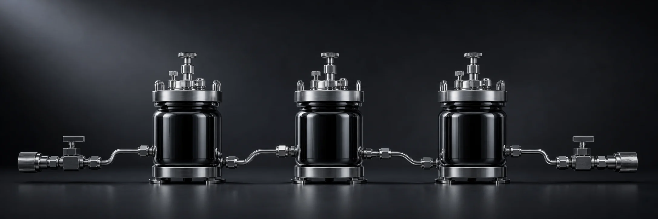
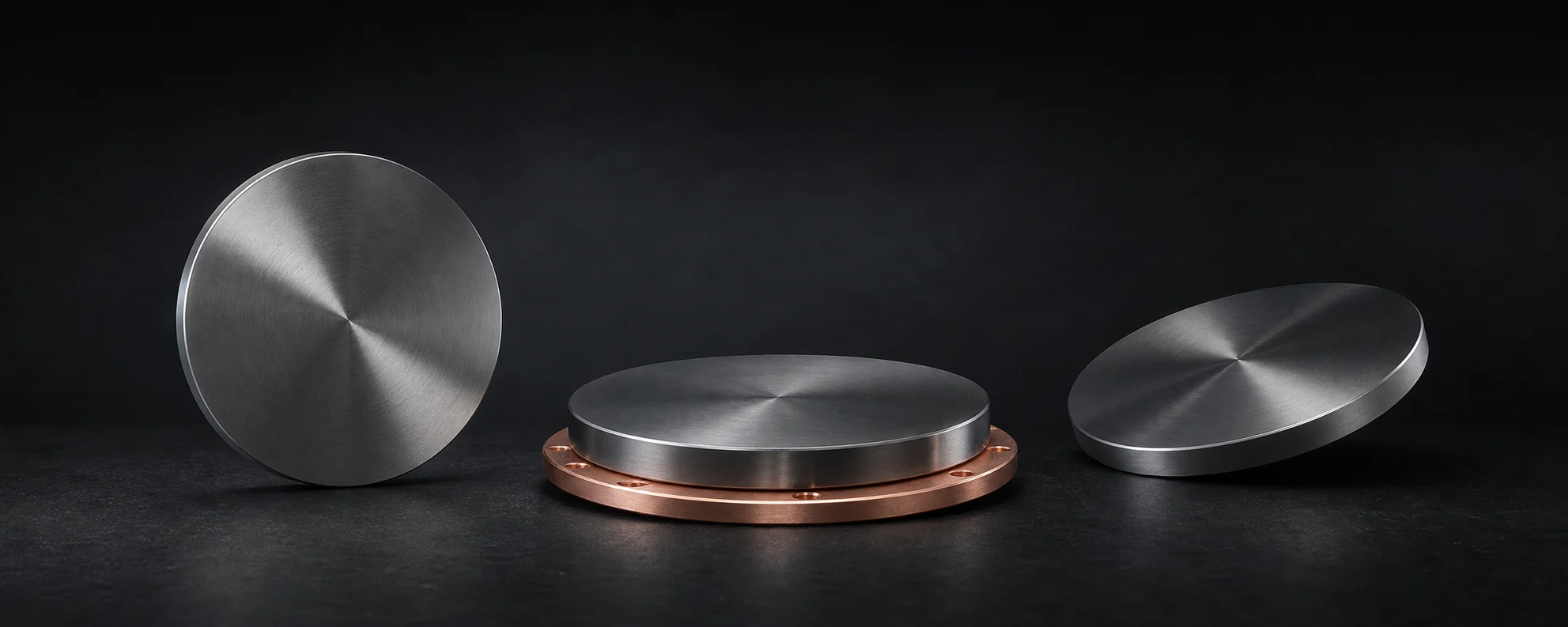
진공 챔버에서 플라즈마 이온이 스퍼터링 타깃 표면을 충돌합니다. 방출된 원자는 진공을 지나 유리, 웨이퍼 또는 기판 위에 재배열되어 나노미터에서 마이크로미터 두께의 기능성 박막을 형성합니다.
Inside a vacuum chamber, ions in a plasma strike a sputtering target. Atoms are released, travel through the vacuum, and rearrange on glass, wafers, or other substrates to form functional films only nanometres or micrometres thick.
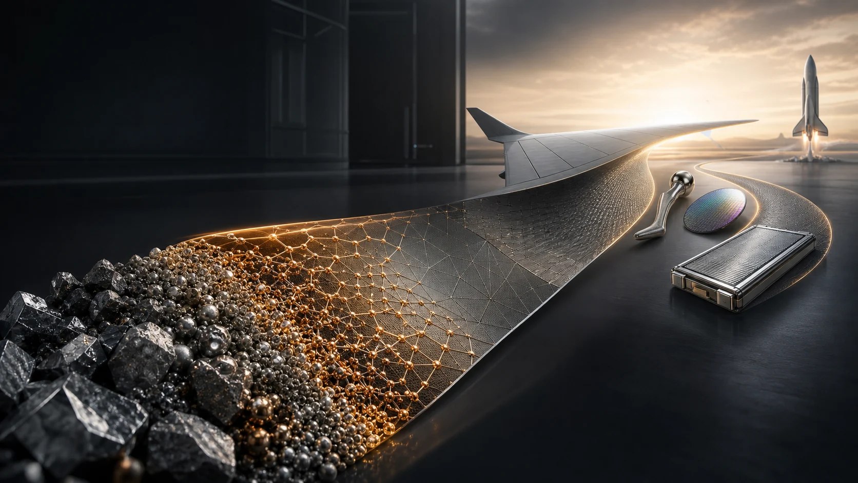
이 박막은 디스플레이의 투명 전도층과 전극, 반도체의 도전·배리어 구조, 빛을 제어하는 광학 코팅과 데이터 저장 및 정밀 센싱용 자성막이 됩니다.
These films become transparent conductive layers and electrodes in displays, conductive or barrier structures in semiconductors, optical coatings that guide light, and magnetic films used in data storage and precision sensing.