
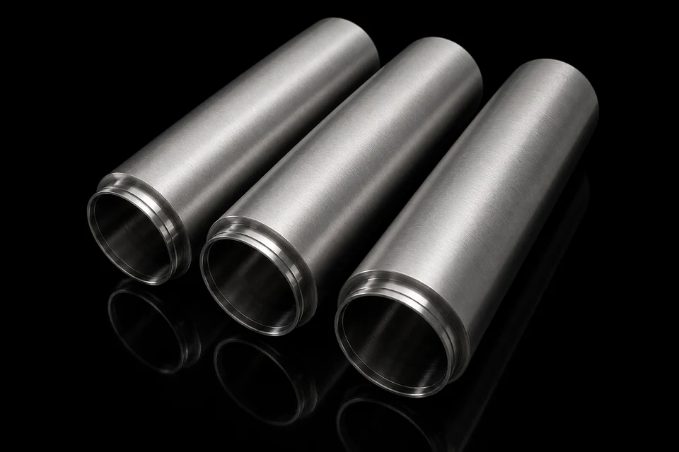
PVD Coating Materials / Sputtering Targets
Ytterbium Metal Target
Specifications
| Product Name | Ytterbium Metal Target |
|---|---|
| Product Line | PVD Coating Materials |
| Category | Sputtering Targets |
| Formula / Composition | Yb |
| Purity | Yb/TREM:99.99%~99.995% |
| Standard Size | Round Target Dia < 350mm; Rectangular Target Width < 240mm; Rectangular Target Length < 550mm; Tube Target OD < 300mm |
| Packaging | Vacuum packaging |
| Customization | Yes |
Product Features
Prepared from high-purity feedstock under controlled processing for stable and uniform thin-film deposition.
Applications
High-purity ytterbium sputtering targets are mainly used for OLED flexible-screen EIL, composite cathodes, and tandem charge-generation layers, reducing power consumption, improving brightness, and extending foldable-screen lifetime while supporting Mini/Micro LED pixel interface coatings. They are also used for advanced semiconductor ohmic contact layers, MRAM magnetic storage films, optical communication laser gain films, and perovskite photovoltaic buffer layers, covering infrared optics, quantum computing, superconductivity, and advanced coating research.
RFQ Checklist