
PVD Coating Materials / Sputtering Targets
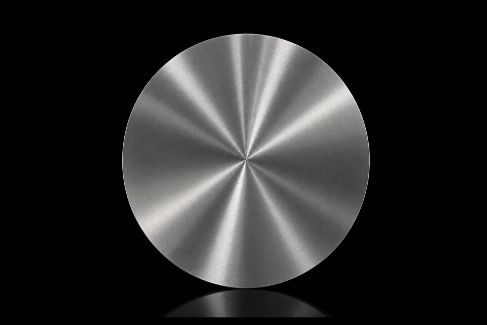
Erbium Metal Target
Specifications
| Product Name | Erbium Metal Target |
|---|---|
| Product Line | PVD Coating Materials |
| Category | Sputtering Targets |
| Formula / Composition | Er |
| Purity | Er/TREM:99.9%~99.95% |
| Standard Size | Round Target Dia < 350mm; Rectangular Target Width < 240mm; Rectangular Target Length < 550mm; Tube Target OD < 300mm |
| Packaging | Vacuum packaging |
| Customization | Yes |
Product Features
Prepared from high-purity feedstock under controlled processing for stable and uniform thin-film deposition.
Applications
Used for erbium-doped optical amplification films in optical communication photonic chips, including EDFA and on-chip waveguides, as well as infrared passive optical device coatings and quantum optical conversion films. Because erbium ions have long coherence lifetimes, the material is suitable for microwave-to-optical quantum signal conversion films and quantum communication chip research.
RFQ Checklist